
The Story So Far...

In a previous article we used the Altronics MegaBox to create a prototype multiprotocol servo/ESC tester. We will build on the techiques and code from that article to create a custom Arduino UNO shield which can be used to deliver the same functionality. As the UNO uses a different microprocessor to the Mega 2560, we may need to change some of the timer and register specific code (actually it turns out only minor changes are required - our PWM output D9 uses Timer 1, which is the same as D11 on the Mega).
The Arduino Shield
Using Fritzing we designed a simple 2 layer Arduino shield (Figure 1) to make it easier to test our hardware. We have made a few changes to our prototype. To save cost we are using a 10k potentiometer in place of the encoder (this saves one digital input as well). We have also replaced the LCD with a version that is controlled via I2C (saving another 5 digital inputs). PWM is being driven via D9. The board has five male header pins in the standard servo connection configuration. This allows you to control up to 4 servo/ESC's (current permitting) and still have an extra connection to view the output on an oscilloscope (for example).

Figure 1. ESC/Servo Tester Shield
As the shield will cover the reset button on the UNO, we have provided another one on the shield. An External Reset is generated by a low level on the RESET pin. In case the other pin connections are not obvious from Figure 1, here are the Arduino UNO pin defintions that you will need.
//PIN CONNECTIONS

//  POTENTIOMETER INPUT
const byte POT = A0;

//  PWM OUTPUT
const byte PWM = 9;

//  PUSH BUTTON INPUTS
const byte PB_DEC = 8;          // Decrement button
const byte PB_INC = 7;          // Increment button
const byte PB_SLT = 6;          // Select Button
const byte PB_BCK = 5;          // Back Button

//END PIN CONNECTIONS
Following testing we will design a 3D printed case for our tester. The LCD is a bit wider than the UNO PCB and we need to allow access to the buttons on the shield.
Parts List
I used the parts in Figure 2, there is nothing special required, but you need to ensure that the dimensions of the parts you select are correct for the PCB design. The part numbers and prices are from Jaycar (these are in AUD and subject to change).

Figure 2. Parts List
In addition to the parts listed above you will need an UNO (or an equivalent clone), a plugpack to power the UNO, the shield PCB, 4 x male to female Dupont cable (Figure 4) and an I2C capable 16 x 2 LCD (Figure 3).
Note that the DPDT switch isn't used in this version of the shield (a subsequent version will include a connection for external power for the servo/ESC's).
I2C Serial 16 x 2 LCD Module
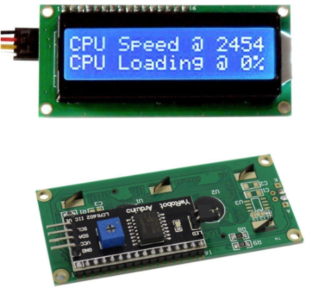
Figure 3. I2C capable LCD 16 x 2
You can buy one of these LCD's online from places like Aliexpress, at the time of writing they were available for USD2.53 (again, this will change). The LCDs are usually attached to another module which performs the serial to parallel conversion using a Philips/NXP PCF8574T. You may have to solder this module on yourself (I did).
The four LCD connection pins (GND, 5V, SDA and SCL) line up with the corresponding connection on the PCB and you could straighten the pins and solder it in place but then you wouldn't have access to the push buttons on the shield or the contrast pot on the back of the LCD. A better option is to use some male to female Dupont cable (Figure 4).

Figure 4. Male to Female Dupont Cable
This link will allow you to download an I2C LCD Arduino Library, which you will need when we develop the firmware in the next section.
The Firmware
The ATmega328P has 6 PWM outputs, 2 are located on each timer/counter. Each timer has two Output Compare Registers (OCR) that control the PWM width for the timer's two outputs. The PWM capable pins are normally marked with a "~" on the UNO and we have replicated this on our shield (Figure 1). The relation between timers and PWM outputs is:
- Timer 0 controls Pins 5 and 6;
- Timer 1 controls Pins 9 and 10; and
- Timer 2 controls Pins 11 and 3.
We are using D9 to deliver our PWM signal, this is on Timer 1 and the relevant OCR for this pin is OCR1A (refer to Figure 9 in the ATmega2560 article). The settings we put in place will effect D10 as well.
To assign D9 as an output, we need to know which Port it is mapped to (or just use pinMode). For the UNO:
- Port B controls digital pin 8 to 13;
- Port C controls the analog input pins; and
- Port D controls digital pins 0 to 7.
From the Arduino pin mapping diagram (Figure 5), we see that digital input 9 (D9) is controlled by bit 1 of Port B's Data Direction Register (DDR). The DDR determines whether a pin is an input or an output (Figure 6).

Figure 5. ATmega168/328P Arduino Pin Mapping

Figure 6. Port B Data Direction Register Bits
Thus we set the DDR of Port B, bit 1 to assign D9 as an ouput:
DDRB |= 1 << DDB1;
Alternatively, you can just use:
pinMode(9, OUTPUT);
As with the ATmega2560, the 328P PWM is capable of running in 3 different modes: Fast PWM, Phase Corrected PWM and Phase and Frequency Phase Corrected PWM.
Every PWM square wave has a duty cycle. This is defined as:
Duty Cycle = [ON time / (ON time + OFF time) ] * 100
We can manipulate the Output Compare Register (OCR) mentioned above, to adjust the PWM duty cycle. The OCR's (A and B) for Timer 1 are 16 bit registers. So for example, to get a 50% duty cycle, you set the OCR to half of the top counter value - referred to as "TOP" in the datasheet. The TOP value can be assigned to be one of the fixed values: 0xFFFF, 0x00FF, 0x01FF, or 0x03FF, or to the value stored in the OCRnA or ICRn Register. The assignment is dependent on the mode of operation.
Fast PWM using Registers
In Fast PWM mode, the timer repeatedly counts from 0 to 255. The output turns on when the timer is at 0, and turns off when the timer matches the output compare register. The higher the value in the output compare register, the higher the duty cycle.
To get hardware PWM working on a pin, you need to as a minimum:
- Set that pin as an output;
- Set the PWM mode and frequency using the Timer Counter Control Registers (TCCR); and
- Set the Output Compare Register to determine the pulse width / duty cycle.
So let's move on to steps 2 and 3. Firstly, there are two TCCR's (A and B). The control bits for TCCR1A are shown in Figure 7.

Figure 7. TCCR1 (A and B) Control Bits.
For fast PWM, we want non-inverting mode, thus from Figure 8, COM1A = 10 (BINARY).

Figure 8. Compare Output Mode Options, Fast PWM.

Figure 9. Waveform Generation Mode Bit Description.
Next we need to set the Waveform Generation Mode. We will use mode 5 (Fast PWM, 8 bit) which has a TOP = 0x00FF = 255. To get mode 5 (ref: Figure 9), we need to set the following bits within the TCCR's:
WGM10:3 = 0101
We will also set the Clock Select (CS) Bits (Figure 10) to set the prescaler to 1. The appropriate value for this is:
CS10:2 = 001

Figure 10. Clock Select Bits.
The Fast PWM frequency for the output can be calculated by the following equation:

The N variable represents the prescaler divider (1, 8, 64, 256, or 1024). For our settings:
fPWM = 16 Mhz / (1 * (1 + 255) = 16000000 / 256 = 62.5 kHz.
The register code to achieve the register operations explained above is as shown in Figure 11.
DDRB |= 1 << DDB1;                // Set D9 as an output pin
TCCR1A = 0;                              // Clear TCCR A & B bits
TCCR1B = 0;
TCCR1A = (1 << COM1A1) | (1 << WGM10);
TCCR1B = (1 << WGM12)  | (1 << CS10);
OCR1A = 127;                             // 50% Duty Cycle (i.e. 127/255)
Figure 11. Fast PWM using Registers.
Measuring the results on our protocol analyser provides the expected outcome (Figure 12), 50% duty cycle, pulse width 8 µs and frequency 62.5 kHz. The pulse width is a product of the duty cycle and the frequency (as period is the inverse of frequency).

Figure 12. Fast PWM Output on D9.
Changing PWM Frequency using Registers
Coincidently, the PWM pin (D9) that we chose on the UNO uses the same timer as the D11 pin on the Mega2560, so apart from the pin output definitions the code for phase and frequency correct PWM is the same (Figure 13). The article on the ATmega2560 version explains why we selected the control register bits in Figure 13. It also explains more about how phase and frequency correct PWM differs from Fast PWM. Of course you can also refer to the ATmega328P data sheet.
DDRB |= 1 << DDB1;                 // Set D9 as an output pin
TCCR1A = 0;                              //  Clear TCCR A & B bits
TCCR1B = 0;
TCCR1A = (1 << COM1A1);                  //  Non-inverting output
TCCR1B = (1 << WGM13)  | (1 << CS11);    //  Phase & Freq correct PWM, prescaler N = 8
ICR1 = 20000;                            //  Freq = 50 Hz
OCR1A = 1500;                            //  pulse width = 1500 us;
Figure 13. Phase & Frequency Correct PWM on the UNO.
The default PWM mode, set by init() in the Arduino boiler plate code, for Timer 1 is mode 1 and we want mode 8 (PWM, Phase and Frequency Correct) - see Figure 9. In mode 8 we can adjust the PWM frequency using register ICR1. To get mode 8 we just set the WGM13 bit. We will use a non-inverting output as before so set the COM1A1 bit in TCCR1A. We set the prescaler (N) to 8, to do this, the CS11 bit in TCCR1B needs to be ON.
From the data sheet, the frequency formula for phase and frequency correct PWM is:

For our settings, the calculation is:
fPWM = 16 MHz / (2 * 8 * ICR1) = 16000000 / (2 * 8 * 20000) = 50 Hz
From this formula, it is apparent that we can adjust the PWM frequency by adjusting the value in register ICR1. It also explains why we use a prescaler of 8. The system clock is 16 MHz and to get the PWM frequency we divide by 2N. If we make 2N = 16 then the relationship between fPWM and ICR1 (i.e. TOP) is straight forward. Rearranging the formula:
ICR1 = 1MHz / fPWM
For a fPWM of 50 Hz, ICR1 = 1,000,000 / 50 = 20,000.

Figure 14. Phase & Frequency Correct PWM waveform at 50 Hz.
The results of the code in Figure 13 is shown in Figure 14. So for our tester we can adjust the pulse width using the value of register OCR1A and we can adjust the PWM frequency using ICR1.
Servo Tester Firmware
We previously used a rotary encoder to select menu options and adjust the PWM pulse width. This functionality is now provided by a 10k linear potentiometer (i.e. variable resistor).
The Arduino ATmega328P has a 10-bit ADC which means it can return 2¹⁰ (i.e. 0–1023) values. This is where the 1024 comes from in the equation from the data sheet:
ADC = (Vin * 1024)/Vref
If you want to convert the ADC value to a voltage use the following formula (as the hardware rounds down):
float voltage = ((float) rawADC + 0.5 ) / 1024.0 * Vref;
I have written a separate article on Programming the ATmega328P ADC Registers which goes into a lot more detail if you are interested but for our purposes we only care about the relative position of the potentiometer so we can just analogRead() the input connected to the middle pin of the potentiometer. The other two pins on the pot are connected to GND and 5V so moving the pot shaft should give us a value between 0 and 1023. The schematic looks like Figure 15.

Figure 15. 10K Potentiometer Connected to an UNO
To test this we can use the sketch shown in Figure 16. As expected, rotating the potentiometer shaft caused the analog input read to vary between 0 and 1023.
#include <Wire.h>
#include <LiquidCrystal_I2C.h>

// Set the LCD I2C address to 0x3F with 16 chars and a 2 line display
LiquidCrystal_I2C lcd(0x3F, 16, 2);

//PIN CONNECTIONS

//  POTENTIOMETER INPUT
const byte POT = A0;

//END PIN CONNECTIONS

void setup() {
  lcd.begin();                    // Initialize the LCD
  lcd.backlight();                // Turn on the backlight
}

void loop() {
  // Read A0
  int potValue = analogRead(POT);

  lcd.clear();
  lcd.print("Pot Value: ");
  lcd.setCursor(0, 1);
  lcd.print(potValue);
  delay(100);                   //  Reduce LCD flicker
}
Figure 16. Potentiometer Test Sketch.
To convert the potValue to a PWM pulse width, we can use the Arduino map() function. You can define the minimum and maximum pulse widths to whatever values you like. I used 800 and 2200.
pulseWidth = map(potValue, 0, 1023, MIN_PULSE_WIDTH, MAX_PULSE_WIDTH);
I have updated the UNO code to provide the same functionality as the Mega 2560 version. The full source listing of the Arduino code is available for download from the Reefwing Gist. In the articles following we will design a 3D case and add additional digital protocols.
No comments:
Post a Comment